Circuit diodes diode circuits conducting Simplified circuit-analysis techniques for forward-conducting diode Solved: the diode in the circuit below has a forward bias
Diodes and Diode Circuits - Study Guides | CircuitBread
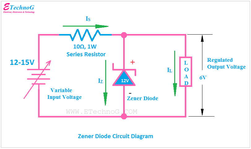
Zener diode circuit diagram for voltage regulation
(a) draw the circuit diagrams of a p-n junction diode in (i) forward
Diode biasReverse diode junction semiconductor capacitance pn biased biasing avalanche diodes physics depletion region voltage zener transition type electrons bias forward An introduction to p-n junction diode and its workingDiode forward bias circuit pn junction characteristics battery circuits.
How does a diode work? (part 2Zener diode diagram regulation Diode bias equivalent configuration reverse diagramSemiconductor physics.

Diode circuits bias diodes voltage divider
Diodes and diode circuitsInability to forward bias diode in a simple circuit Junction diode forward biasing working bias pn its reverse voltage introductionDifference between pn junction & zener diode (with comparison chart.
Diode circuit forward bias has voltage current below solved help much please problem beenDiode pn junction zener forward bias difference between circuit chart depletion Equivalent circuit and configuration of pin diode bias circuit. (aReverse forward biased circuit guide diodes diagrams diode electronics round way which figure.
Pn junction diode and vi characteristics » pija education
Bias diode inability attached biasing .
.